
2010 Robert Finch
![]()
Overview
bcPSG is a audio interface circuit for use within a programmable system to interface the system to an audio output. It supports four ADSR audio channels with a wavetable option.
* The core has been tried and found to produce reasonable output (see Butterfly System project).
Digitally programmable audio Interface Circuit with the following features:
|
programmable wave table memory address | |
|
four ADSR / wave table channels (0-3) | |
|
programmable frequency and pulse width control, | |
|
0.06 Hz frequency resolution | |
|
attack, decay, sustain and release | |
|
test, ringmod, sync and gate controls | |
|
five voice types: triangle, square, pulse, noise and wave | |
|
exponential decay and release |
Dowload Source: Ask!
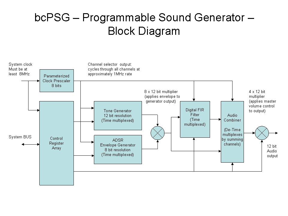
Block Diagram: bcPSG.gif
Notes:
The Master port signals may be left unconnected if the wave table option is not required. This will not reduce the size of the core.
Since the wave table isn't large (16kB max), it may be desirable to interface the Master port directly to one side of a dual port memory, and the system to the other side. Otherwise an external bus arbitrator will be required.
It is possible to use a smaller wave table memory. For example it may be neccessary to support only a single channel (4kB).
Core Stats (subject to change):
Spartan3 - Webpack 9.1i xc3s1000-4ft256
975 LUTs / 650 slices / 60MHz3 multipliers
(uses <10% of a xc3s1000)
![]()
Module Interface Description
bcPSG16
module
bcPSG16(rst_i,
clk_i, cyc_i, stb_i, ack_o, we_i, adr_i, dat_i, dat_o,
vol_o, o);
parameter pClkDivide;
parameter pAddress;
| Signal | Description |
| rst_i | This signal is normally connected to the system reset signal. It resets the sound generator interface forcing it to the reset state. |
| clk_i | This is usually connected to the system clock and is used as a base timing clock. This clock should be at least 8MHz to ensure proper operation. |
| Slave Port Signals | |
| cyc_i | indicates that a valid bus cycle is taking place. The core will not respond to the bus unless this signal is active. |
| stb_i | This strobe signal also indicates that a valid bus cycle is taking place |
| ack_o | This signal indicates that the core has processed the bus transaction (it is the logical and of cyc_i and stb_i). |
| we_i | This signal is used to signify a write operation to the PSG. |
| adr_i | This seven bit address bus is used to address one of PSG's registers. (Registers are described below). |
| dat_i | This is the sixteen bit data input bus to the PSG. |
| dat_o | This is the sixteen bit data output bus from the PSG. |
| vol_o | Volatile data output indicator. Indicates that the value from the core should override I/O shadow memory. |
| Master Port Signals (for wave table reading) | |
| m_cyc_o | Indicates that a valid bus cycle is taking place. The core is not requesting the bus unless this signal is active. |
| m_stb_o | This strobe signal also indicates that a valid bus cycle is taking place |
| m_ack_i | This input signal indicates to the core that the system has processed the bus transaction. |
| m_we_o | This signal is supplied to the system in a fixed inactive state to indicate that the master access is a read access. |
| m_sel_o | This two bit signal bus indicates which byte lanes need to be read during a master access. Both select lines are automatically driven during an access, resulting in a 16 bit read. |
| m_adr_o | This 32 bit address bus is used to supply the address for the wave table access. The lower twelve bits are driven by the tone generator counters. Limiting the wave table size to 4kB for each channel. The upper bits are supplied by a control register. |
| m_dat_i | This is the sixteen bit data input bus to the PSG. Only 12 bits are read. |
| o | This the 12-bit audio output value from the core. It will need to be driven into a digital-to-analog converter of some sort. |
| Parameters | |
| pClkDivide | Use this parameter to specify the clock prescale divider value. The core expects to work with an internally generated cycle of about 1MHz. The default setting of 66 assumes a 66MHz system clock. |
| pAddress |
This parameter sets the system address that the core responds to. The default setting is $FFD0_00xx |
![]()
Register Description
| Reg. No. | 15 0 | Function | Description |
| 0 | nnnnnnnn nnnnnnnn | channel 0 frequency | contains sixteen bits of
the note frequency for channel zero. freq = n * 0.06 Hz |
| 1 | ---- nnnn nnnnnnnn | channel 0 pulse width low | contains twelve bits of the pulse width for channel zero. |
| 2 | trsg --fo - vvvvv -- | channel 0 control | 5 bits used to control the voice type
for the channel bit 6 = wave table 1 = on, 0 = off bit 5 = noise bit 4 = pulse bit 3 = square wave bit 2 = triangle wave
bit 15 = test bit 14 = ring mod bit 13 = sync bit 12 = gate bit 8 = output enable bit 9 = 1 = rout to filter
|
| 3 | -------- -------- | reserved | this register is not used |
| 4 | nnnnnnnn nnnnnnnn | channel 0 attack rate | 16 bits used to control the attack rate of the envelop generator. Rate varies from 0 to 15.6 s in linear steps. Each step is 977.8 ns. |
| 5 | ---- nnnn nnnnnnnn | channel 0 decay rate | 12 bits used to control the decay rate of the envelop generator. Decay is exponential. Varies from 0 to 32s. |
| 6 | -------- nnnnnnnn | channel 0 sustain level | 8 bits used to determine the sustain level of the envelop generator |
| 7 | ---- nnnn nnnnnnnn | channel 0 release rate | 12 bits used to control the release rate of the envelop generator. Release is exponential. Varies from 0 to 32s. |
| 8 - 31 | channels one through three, identical to channel zero | ||
| 32 - 63 | reserved for channels four through eight, identical to channel zero | ||
| 64 | -------- ---- vvvv | master volume control | 4 bit value used to control the master volume, varies linearly between 0 and 15 |
| 65 | nnnnnnnn nnnnnnnn | note generator 3 output | 16 bit value reflecting the output of note generator #3 |
| 66 | -------- nnnnnnnn | envelope generator 3 output | 8 bit value reflecting the output of envelope generator #3 |
| 68 | a ------- -------- | wave table base address low |
bit 15 of the wave table address bits 14-12 are determined by the channel number bits 11-0 come from the frequency accumulator for the channel |
| 69 | aaaaaaaa aaaaaaaa | wave table base address high | contains bits 16 to 31 of the wave table address |
| 80 - 95 | s --- kkkk kkkkkkkk | filter coefficients |
filter coefficients for 16 tap fir filter stored in sign-magnitude format s = sign k = 12 bit coefficient |
![]()
The bcPSG16 core may be directly interfaced to a WISHBONE compatible bus.
|
WISHBONE Datasheet WISHBONE SoC Architecture Specification, Revision B.3 |
||
|
|
|
|
|
Description: |
Specifications: |
|
|
General Description: |
PSG - Programmable Sound Generator |
|
|
Supported Cycles: |
SLAVE, READ / WRITE SLAVE, BLOCK READ / WRITE SLAVE, RMW |
|
|
Data port, size: Data port, granularity: Data port, maximum operand size: Data transfer ordering: Data transfer sequencing |
16 bit 16 bit 16 bit Little Endian any (undefined) |
|
|
Clock frequency constraints: |
Minimum 8MHz input clock frequency. Maximum 255 MHz input clock. |
|
|
Supported signal list and cross reference to equivalent WISHBONE signals |
Signal Name: ack_o adr_i(31:0) clk_i dat_i(15:0) dat_o(15:0) cyc_i stb_i we_i |
WISHBONE Equiv. ACK_O ADR_I() CLK_I DAT_I() DAT_O() CYC_I STB_I WE_I
|
|
Special Requirements: |
|
|